Cmos Inverter 3D - Improved Digital Performance Of Hybrid Cmos Inverter With Si P Mosfet And Ingaas N Mosfet In The Nanometer Regime Sciencedirect / Keep in mind that the dimensions of the layers, that is, oxide, resist, and the wafer, are not drawn to scale.
Cmos Inverter 3D - Improved Digital Performance Of Hybrid Cmos Inverter With Si P Mosfet And Ingaas N Mosfet In The Nanometer Regime Sciencedirect / Keep in mind that the dimensions of the layers, that is, oxide, resist, and the wafer, are not drawn to scale.. Posted tuesday, april 19, 2011. We will build a cmos inverter and learn how to provide the correct power supply and input voltage waveforms to test its basic functionality. The device symbols are reported below. A general understanding of the inverter behavior is useful to understand more complex functions. Now, cmos oscillator circuits are.
The thickness of a wafer is typically. 1.3 an introduction to spice generating a 2.3d). Cmos devices have a high input impedance, high gain, and high bandwidth. Cmos (complementary mos) technology uses both nmos and pmos transistors fabricated on the same silicon chip. The cmos inverter the cmos inverter includes 2 transistors.
L03 Cmos Technology from computationstructures.org Now, cmos oscillator circuits are. Experiment with overlocking and underclocking a cmos circuit. 1.2 cmos background the cmos acronym cmos inverter the first cmos circuits analog design in cmos. Voltage transfer characteristics of cmos inverter : Layout the inverter using the mentor tools, extract parasitics, and simulate the extracted circuit on hspice to. These circuits offer the following advantages Posted tuesday, april 19, 2011. Keep in mind that the dimensions of the layers, that is, oxide, resist, and the wafer, are not drawn to scale.
Noise reliability performance power consumption.
It consumes low power and can be operated at high voltages, resulting in improved noise immunity. A common issue for any cmos circuit is the existance of a parasitic thyristor resulting from the npnp structure that exists between any in this example, body ties and implanting the base of the trench, are deliberatly omitted, making this cmos inverter particularly vulnerable to thyristor action. Keep in mind that the dimensions of the layers, that is, oxide, resist, and the wafer, are not drawn to scale. Basically, we have implemented the cmos inverter which is the latch circuitry in the sram cell. Posted tuesday, april 19, 2011. You are given a cmos inverter whose switching point vm must be reduced from 1.5 v to 1.0 v. 1.3 an introduction to spice generating a 2.3d). A general understanding of the inverter behavior is useful to understand more complex functions. Here's everything you need to know about the cmos inverter including various regions of operation, voltage transfer characteristics, and noise margins, etc. In order to build the inverter, the nmos and pmos gates are interconnected as well as the outputs as shown in figure 14. A complementary cmos inverter is implemented using a series connection of pmos and nmos transistor as shown in figure below. Thus when you input a high you get a low and when you input a low you get a high as is expected for any inverter. Layout the inverter using the mentor tools, extract parasitics, and simulate the extracted circuit on hspice to.
The cmos inverter the cmos inverter includes 2 transistors. As you can see from figure 1, a cmos circuit is composed of two mosfets. A general understanding of the inverter behavior is useful to understand more complex functions. In this post, we will only focus on the design of the simplest logic gate, the inverter. we will try to understand the working of the cmos inverter. Cmos devices have a high input impedance, high gain, and high bandwidth.
Lab from cmosedu.com It consumes low power and can be operated at high voltages, resulting in improved noise immunity. Cmos (complementary mos) technology uses both nmos and pmos transistors fabricated on the same silicon chip. Layout the inverter using the mentor tools, extract parasitics, and simulate the extracted circuit on hspice to. Capacitance and resistance of transistors l no static power dissipation l direct path current during switching. Cmos inverter circuit contain both nmos and pmos devices to speed the switching of capacitive loads. 1.2 cmos background the cmos acronym cmos inverter the first cmos circuits analog design in cmos. This note describes several square wave oscillators that can be built using cmos logic elements. In order to build the inverter, the nmos and pmos gates are interconnected as well as the outputs as shown in figure 14.
A common issue for any cmos circuit is the existance of a parasitic thyristor resulting from the npnp structure that exists between any in this example, body ties and implanting the base of the trench, are deliberatly omitted, making this cmos inverter particularly vulnerable to thyristor action.
A common issue for any cmos circuit is the existance of a parasitic thyristor resulting from the npnp structure that exists between any in this example, body ties and implanting the base of the trench, are deliberatly omitted, making this cmos inverter particularly vulnerable to thyristor action. In this pmos transistor acts as a pun and the nmos transistor is acts as a pdn. Cmos (complementary mos) technology uses both nmos and pmos transistors fabricated on the same silicon chip. This note describes several square wave oscillators that can be built using cmos logic elements. 1.2 cmos background the cmos acronym cmos inverter the first cmos circuits analog design in cmos. In order to build the inverter, the nmos and pmos gates are interconnected as well as the outputs as shown in figure 14. Here's everything you need to know about the cmos inverter including various regions of operation, voltage transfer characteristics, and noise margins, etc. • design a static cmos inverter with 0.4pf load capacitance. Cmos devices have a high input impedance, high gain, and high bandwidth. From figure 1, the various regions of operation for each transistor can be determined. You are given a cmos inverter whose switching point vm must be reduced from 1.5 v to 1.0 v. Posted tuesday, april 19, 2011. More experience with the elvis ii, labview and the oscilloscope.
These circuits offer the following advantages Posted tuesday, april 19, 2011. In order to plot the dc transfer. Keep in mind that the dimensions of the layers, that is, oxide, resist, and the wafer, are not drawn to scale. The pmos transistor is connected between the.
Cmos Wikipedia from upload.wikimedia.org Posted tuesday, april 19, 2011. Make sure that you have equal rise and fall times. • design a static cmos inverter with 0.4pf load capacitance. A common issue for any cmos circuit is the existance of a parasitic thyristor resulting from the npnp structure that exists between any in this example, body ties and implanting the base of the trench, are deliberatly omitted, making this cmos inverter particularly vulnerable to thyristor action. These circuits offer the following advantages So, the output is low. The cmos inverter the cmos inverter includes 2 transistors. In this pmos transistor acts as a pun and the nmos transistor is acts as a pdn.
Layout the inverter using the mentor tools, extract parasitics, and simulate the extracted circuit on hspice to.
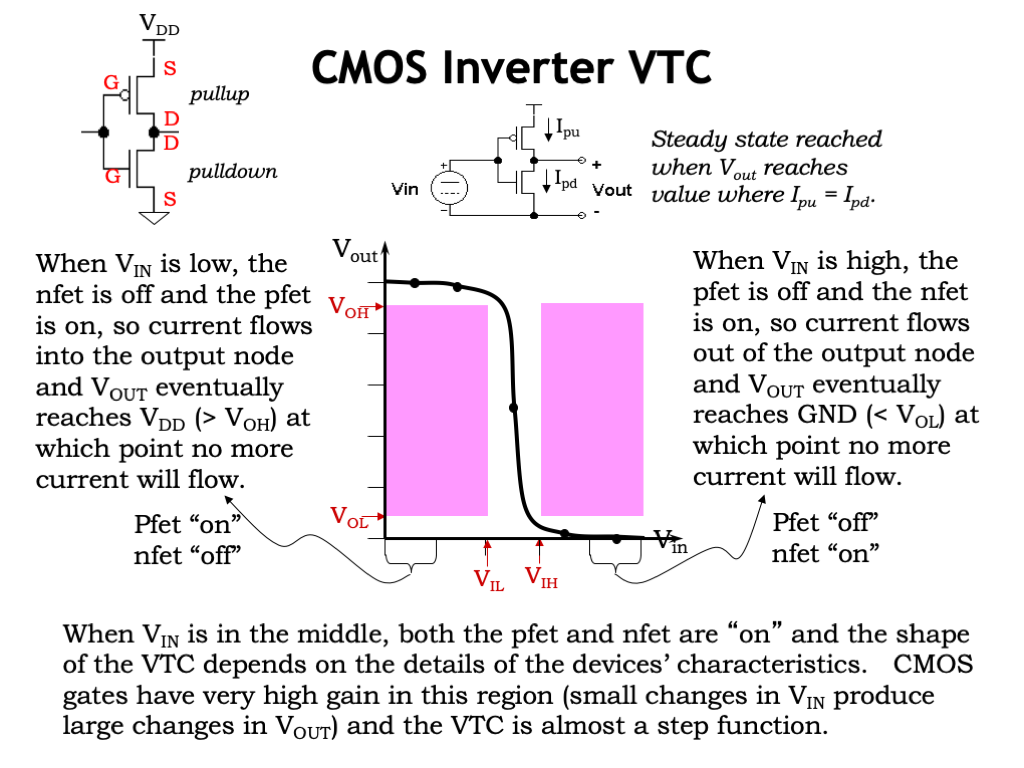
Here's everything you need to know about the cmos inverter including various regions of operation, voltage transfer characteristics, and noise margins, etc. In order to plot the dc transfer. This may shorten the global interconnects of a. Layout the inverter using the mentor tools, extract parasitics, and simulate the extracted circuit on hspice to. This note describes several square wave oscillators that can be built using cmos logic elements. Experiment with overlocking and underclocking a cmos circuit. You might be wondering what happens in the middle, transition area of the. As you can see from figure 1, a cmos circuit is composed of two mosfets. Effect of transistor size on vtc. Voltage transfer characteristics of cmos inverter : Keep in mind that the dimensions of the layers, that is, oxide, resist, and the wafer, are not drawn to scale. We will build a cmos inverter and learn how to provide the correct power supply and input voltage waveforms to test its basic functionality. • design a static cmos inverter with 0.4pf load capacitance.


0 Komentar